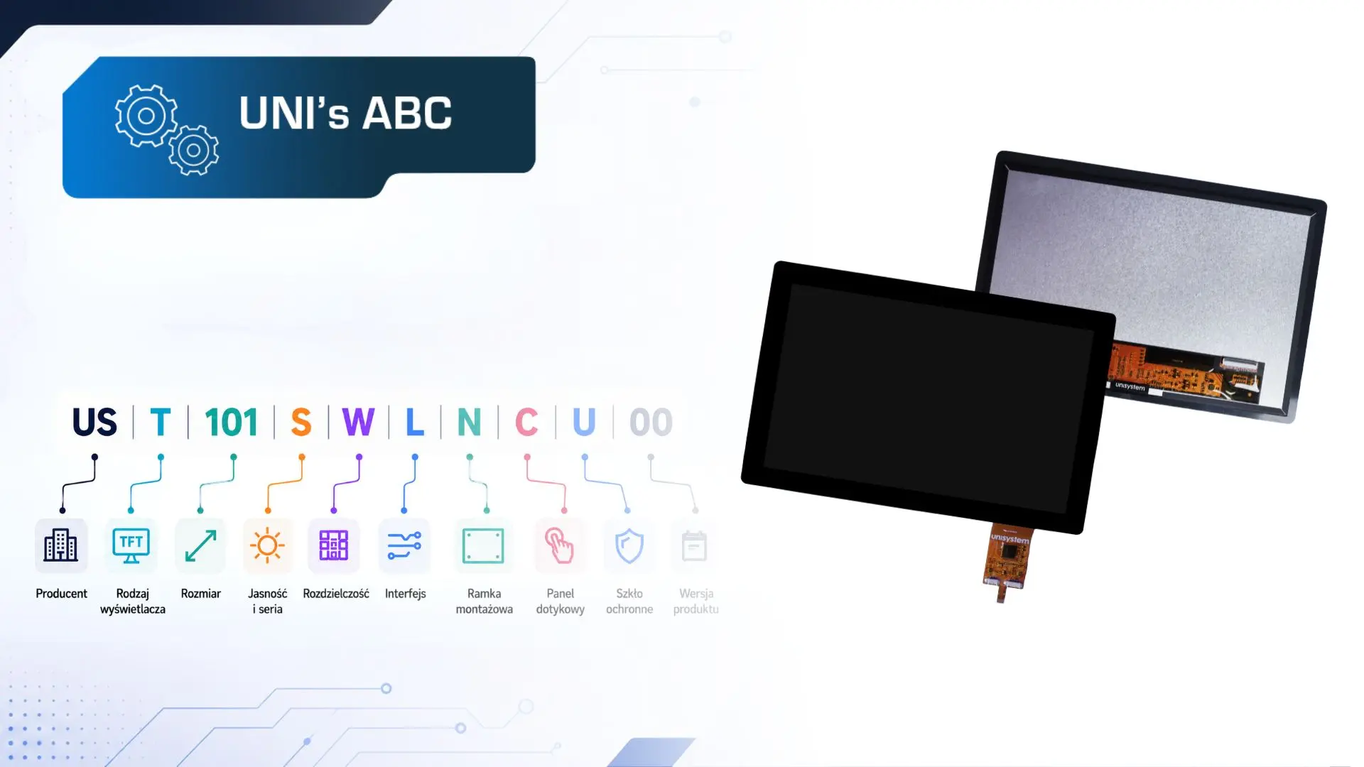
How to Read Unisystem Part Numbers: A Guide to the Lite, Core, and Pro Lines
Unlock the secrets of Unisystem part numbers. Discover how to read them to understand key product features.
Read more →
Display Supplier &
Manufacturer
Knowledge Hub
News, technical articles and insights from Unisystem
Unlock the secrets of Unisystem part numbers. Discover how to read them to understand key product features.
Unlock the secrets of Unisystem part numbers. Discover how to read them to understand key product features.
Evaluate display quality effectively. Discover how to assess a supplier before integration to guarantee consistent performance.
Understand MOQ for display orders: its meaning, dependencies, and impact on project execution and planning.
Displays used in portable, measuring, and battery-powered devices must meet different requirements than conventional screens designed for applications with advanced graphics. Key considerations include not only readability, but also exceptionally low power consumption, stable presentation of static content, and reliable operation under changing lighting conditions. These requirements are met by Winstar’s MIP (Memory in Pixel) […]

Find out how standards for military equipment influence the design and performance of displays across different defence platforms.
For more than three decades, Unisystem has been active in information visualization technologies, supporting manufacturers of electronic devices in the selection, integration, and development of components tailored to specific application requirements. Over the years, our role has gradually evolved – from a component supplier, through a technology partner, to a designer and manufacturer of our […]
Learn how to choose a display for an HMI application by considering technologies, operating conditions, and design requirements.
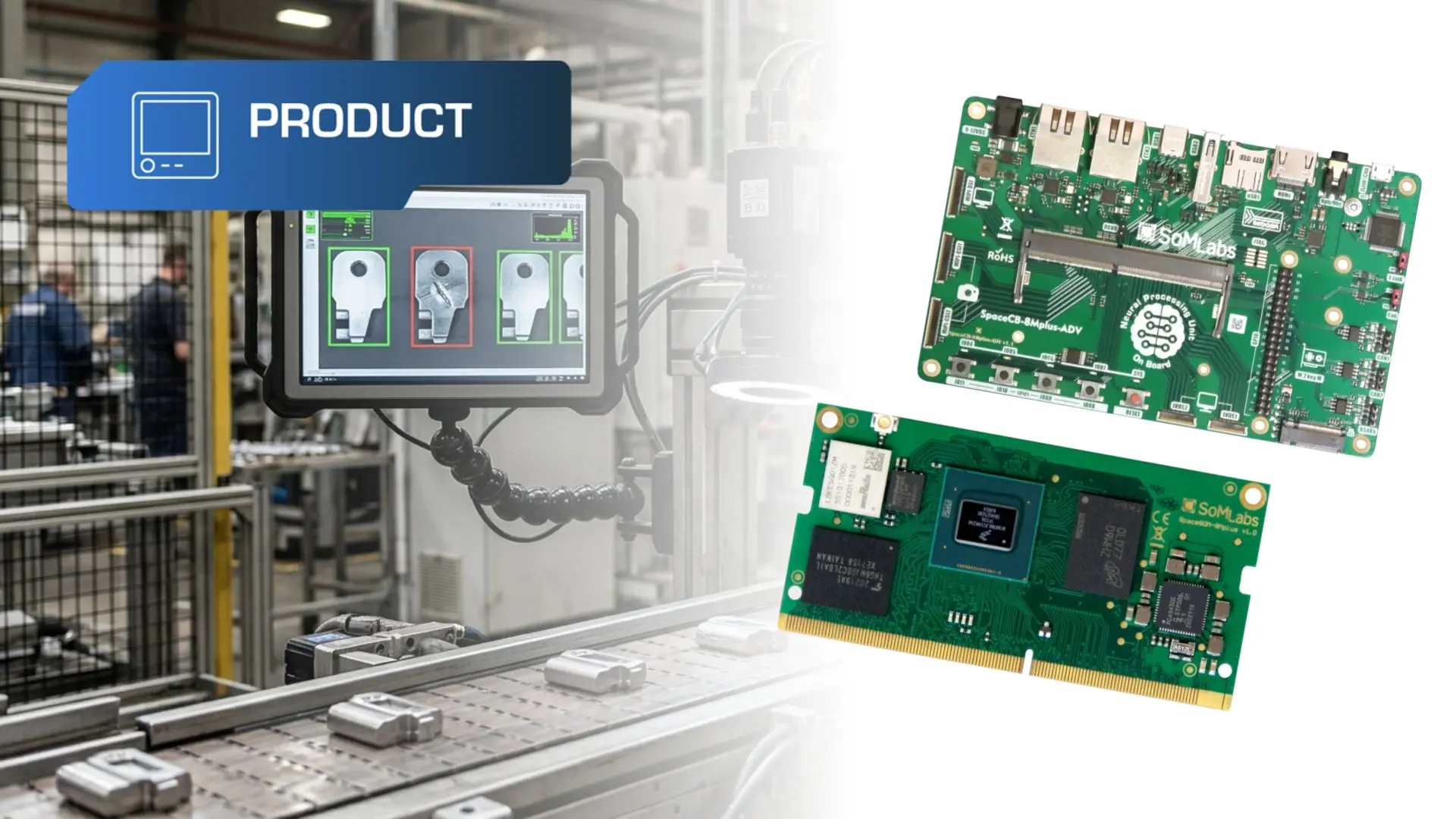
The growth of the Internet of Things, robotics, and artificial intelligence is driving designers to seek hardware platforms that are flexible, energy-efficient, and powerful. Such solutions make it easier to move from concept to testing and integration, while also helping to organize the architecture of the device being developed. This is one of SoMLabs areas […]

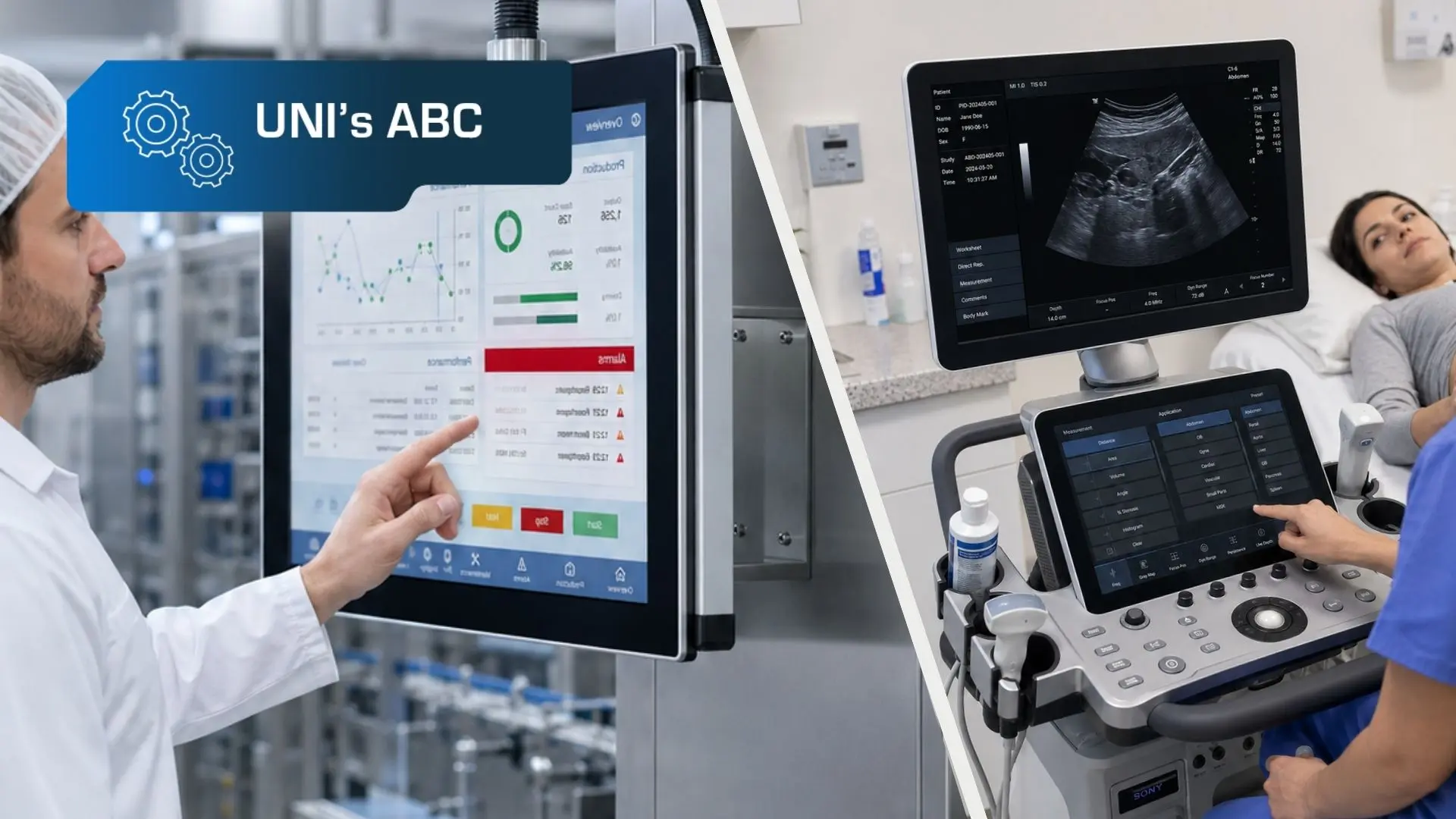
Learn what HMI is in the context of industrial applications, enhancing operator communication and system monitoring.

As industrial digitalization continues to advance, modern human-machine interfaces are becoming increasingly important. A properly selected display affects not only operator ergonomics, but also the reliability of the entire device. The G121ICE-L02 model from Innolux combines the parameters expected from an industrial-grade panel with high readability, offering WXGA resolution (1280 × 800 px), wide viewing […]

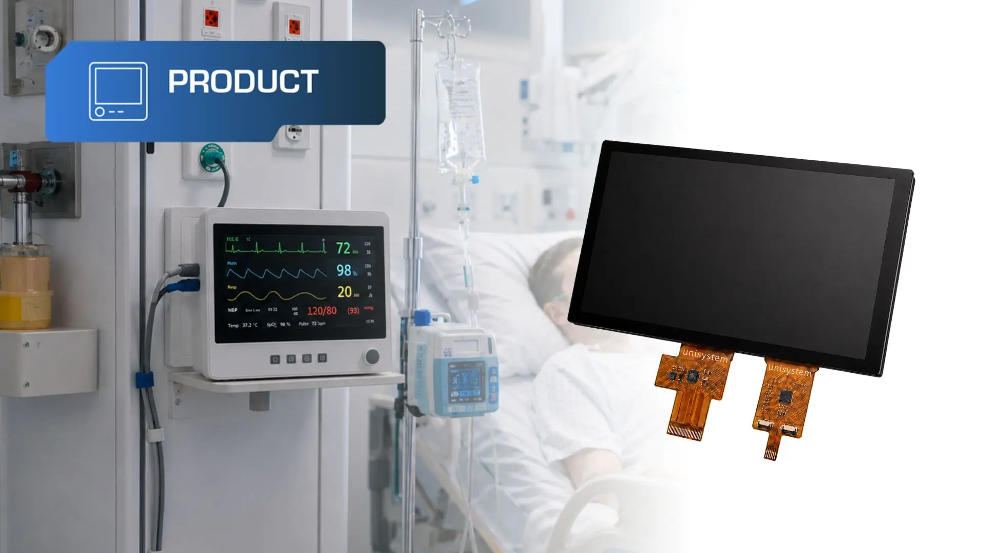
Unisystem is launching its own industrial LCD-TFTs in three product lines: Lite, Core and Pro. The modules have been developed based on 30 years of experience in supplying displays and delivering customized solutions for industrial applications. Jacek Marcinkowski, CTO at Unisystem, discusses their technical specifications, indoor and outdoor use cases, and the competitive advantages of […]

The design of embedded systems is increasingly based on ready-made, proven hardware platforms. This approach helps accelerate product development while reducing implementation risk. Instead of designing the entire electronics architecture from scratch, engineers are increasingly turning to modular solutions, where key functions are divided between specialized system components. This is the idea behind the platform […]